Integrated design and manufacturing services for a broad range of photonic devices including FP & DFB Lasers, SOAs, RSOAs and Detectors. This common design and manufacturing framework for InP photonics devices, uses established and reliable process modules to produce a broad range of device types on 100mm wafers. We have introduced the InP100 platform approach at exactly the point when optical communications and sensing applications require a single-chip, nanoscale solution to meet volume, power, performance and cost demands.
InP100 Product Platform Key Features
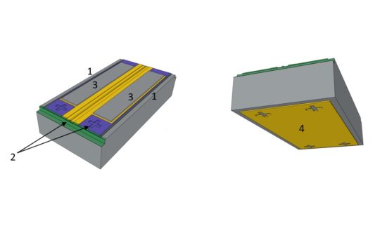
Key design features:
Key design features:
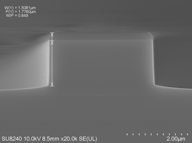
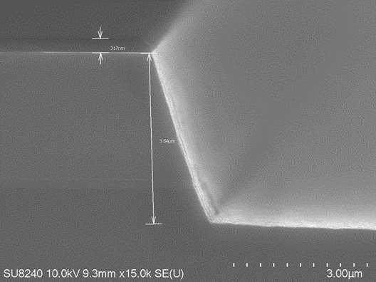
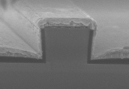
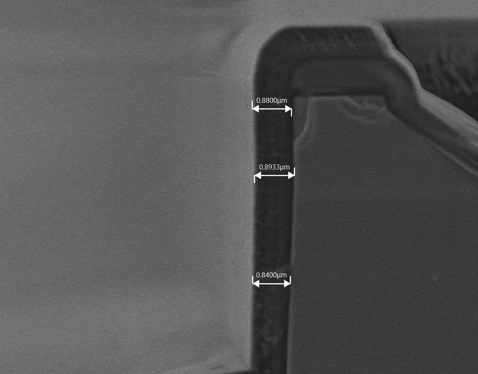
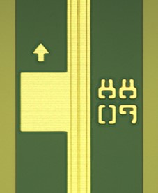
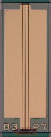
Straight and angled etched facets Vertical and angled etched profiles / Accurate vertical alignment
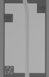
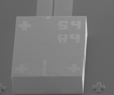
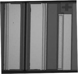
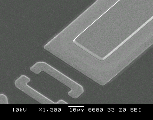
… Self-aligned front-side fiducials .. Back-side alignment fiducials and chip IDs….CV….…. .Optimised low resistance metal stack… .. ..…
Co-planar contacts AuSn solder on III-V On wafer optical coatings
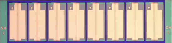
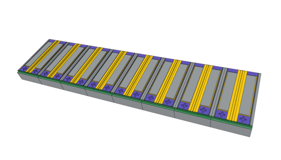
DFB laser diode arrays designed for use in CW-WDM MSA compliant applications

For more information about Sivers Photonics, or to discuss your photonics project requirements.