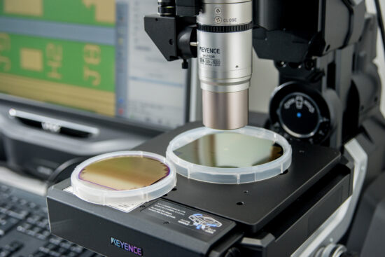
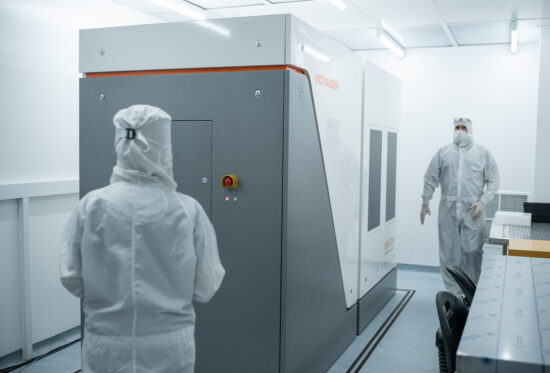
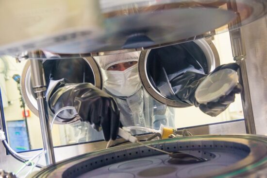
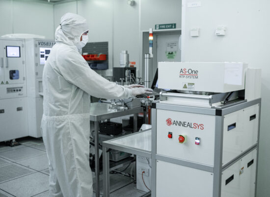
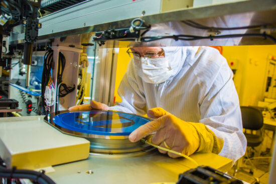
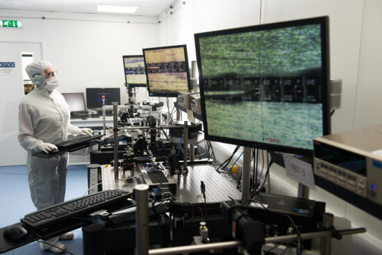
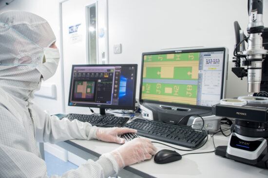
Our foundry provides end-to-end design, manufacture and qualification for early phase prototypes and high-volume production, supporting up to 100mm wafer sizes on InP, GaAs, GaSb and GaN substrates. We have an extensive portfolio of unique production process IP, essential to high-quality, reliable, volume manufacturing.
x
x
x
x
x
x
x
x
x
x
x
x
x
x
x
x
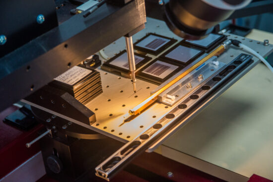
We provide custom mechanical feature optimised for hybrid integration to silicon photonic.
x
x
x
x
x
x
x
x
x
x
x
x
x
x
x
x
We’d love to show you how Sivers Semiconductors can help transform your business—contact us for further information.