![]()
![]()
![]()
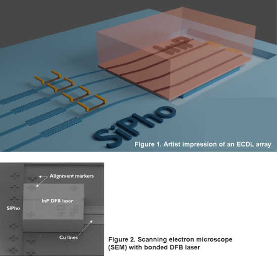
Since the project’s launch in 2019, significant progress has been made in the successful hybrid integration of DFB lasers onto silicon photonics integrated circuits. Reference interface designs and assembly processes have been created for flip-chip bonding DFB lasers from Sivers’ InP 100 product platform, with sub 0.5-μm precision, enabling reproducible coupling losses below 2dB and waveguide-coupled power as high as 40mW.
This integration of DFB lasers into silicon photonic integrated circuits allows for the creation of compact, low-power, and cost-effective devices that can operate at high speeds over long distances and can target a a broad range of applications, including optical communications, optical 3D sensing (LiDAR), biophotonics, high-precision metrology, gas sensing and more.

Finished laser dies operating in the O-band and C-band wavelength ranges are designed, manufactured, and tested by Sivers, ensuring high yield.
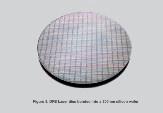
Distributed Feedback (DFB) laser chips bonded on imec’s wafers deliver up to 40mW of optical power coupled to waveguide.
Arrays of reflective semiconductor amplifiers (RSOAs) are also available to realize extended optical cavity diode lasers (ECDLs) with silicon nitride mirrors for O-band and C-band operations.
LEARN MORE ABOUT THE DEVICE TYPES WE OFFER
.
.
.
.
.
.
.

Imec’s silicon photonics technology ‘iSiPP’ is available on 200 and 300mm wafer sizes, including a wide range of active and passive devices.
The interface for flip-chip DFB laser integration has been developed in imec’s iSiPP200N platform. In addition to high-speed electro-optic Si modulators, high-bandwidth Ge photodetectors and efficient thermo-optic heaters, this platform includes highly uniform LPCVD SiN waveguides, enabling low-loss SiN waveguides with accurate phase control, enabling the synthesis of high quality, precise filters and complex circuits.
.
.
.

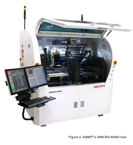
Laser integration is done at wafer scale using the high- precision AMICRA NANO flip-chip bonding tool from ASMPT, with an in-plane alignment capability below 200nm (3σ).
After the flip-chip bonding process and interface design optimization, imec and ASMPT have achieved reproducible post-bonding x-y alignment accuracies of better than 300nm and vertical alignment accuracy of better than 150nm.
The coupling loss between the InP DFB laser facet and the SiN waveguide is consistently better than -2dB, with up to 40mW of optical power coupled into the silicon photonics PIC.
.
.
.
.
.
The combined technology enables you to add multiple infrared light sources to your PIC design, with reference designs available in the O and C-band. Upon request, additional wavelengths can be considered, addressing the fields of optical communications, sensors, computing, or LiDAR applications.
![]()
Figure 5. Left: misalignment measurements along x and
y axis showing a 3σ alignment accuracy below 300 nm.
Right: Laser/SiN waveguide coupling loss before and
after epoxy underfill for different SiN tip widths.
![]()
Figure 6. Microscope picture of a four-channel InP
RSOA chip from Sivers Photonics integrated into an
iSiPP200N wafer.
Thermal Characterisation of Hybrid, Flip-Chip InP-Si DFB Lasers. Published in: Micromachines
David Coenen, Huseyin Sar, Herman Oprins, Aleksandrs Marinins, Yannick De Koninck, Stuart Smyth, Yoojin Ban, Joris Van Campenhout and Ingrid De Wolf
Wafer-Scale Hybrid Integration of InP DFB Lasers on Si Photonics by Flip-Chip Bonding With sub-300 nm Alignment Precision. Published in: IEEE Journal of Selected Topics in Quantum Electronics (subscription required)
Authors: Aleksandrs Marinins , Sebastian Hänsch, Huseyin Sar, François Chancerel , Negin Golshani, Hsiao-Lun Wang, Artemisia Tsiara , David Coenen, Peter Verheyen, Giovanni Capuz , Yannick De Koninck, Ozan Yilmaz, Geert Morthier , Filip Schleicher , Geraldine Jamieson, Stuart Smyth, Andrew McKee, Yoojin Ban, Marianna Pantouvaki, Douglas Charles La Tulipe, and Joris Van Campenhout
For more information about Sivers Photonics, or to discuss your Photonics project requirements.