
High-Power Lasers for Datacenter Optical Interconnects
Delivering precision, scalability and lower power consumption to accelerate next-generation compute infrastructure
Advanced Lasers for AI, HPC, and Beyond
Modern AI and HPC architectures demand optical interconnect solutions that scale in both speed and density. Sivers Photonics’ portfolio of high-power DFB laser chips and arrays provides the foundation for pluggable modules, co-packaged optics, and silicon photonics platforms.
By combining high optical output, stable single-mode operation, and CW-WDM MSA compliance, our solutions enable engineers to design systems that move more data, delivers lower power consumption, and achieve stable performance under real-world operating conditions.
Applications


InP100 Platform
What is the InP100 Platform?
- Standardised InP design and manufacturing platform for 4” wafers
- Supports FP/DFB lasers, reflective SOAs (gain chips), and booster SOAs
- Broad library of epi designs covering 1270–1650 nm
- Etched-facet process with integrated on-wafer optical coatings
Key Advantages
- High yield and proven reliability
- Consistent quality with easy scalability to high-volume production
- Optimised for SiPh flip-chip hybrid integration
- Flexible customization options for power, wavelength, and form factor.
- Faster development cycles and reduced time to market
Product Portfolio
We focus on InP sources optimised for silicon photonics integration. We offer high power, InP-based DFB lasers and gain chips, as single emitters or arrays, on our InP100 Product Platform

FR4 CWDM DFB Chipset
A chipset of 4 x single mode, edge-emitting DFB laser diode chips, designed for CW use in CWDM4 applications with external modulation.
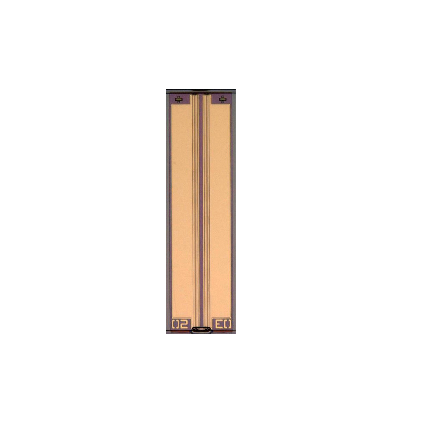
DR8 1310nm 70mW DFB Laser Diode
The 1310nm DFB laser diode operates at a wide temperature range and is designed for 800G and above transceivers
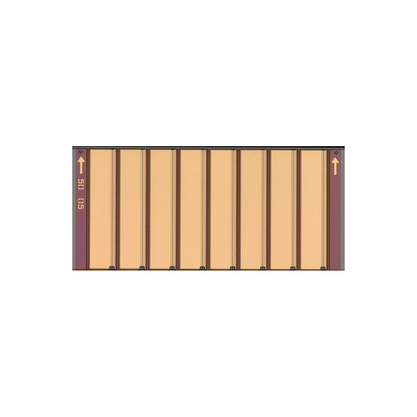
8λ O-band CW DFB Laser Chipset
8 channel edge-emitting DFB laser diode array designed for CW use in CW-WDM-MSA compliant applications.
FAQ
Yes see our product portfolio for a range of standard devices currently underqualification. We can provide you with data sheets, samples and lead times for each.
Don’t see what you’re looking for? Please reach out, our team will be happy to discuss your requirements.
Absolutely. Our in-house design team can take you from initial concept through custom design, prototyping, qualification, and into high-volume manufacturing
InP100 is our 4” Indium Phosphide processing platform – a library of qualified process modules that can be combined to build a wide range of devices.
By using these proven building blocks, InP100 ensures that both established and new design concepts have the strongest chance of success from the start.
There’s no strict minimum. Our goal is to support you from prototyping through to high volumes. We understand every project is unique, so we’ll assess your request individually and build the right plan together.
We run a 24/7 fab and always aim to deliver as quickly as possible. Cycle time varies based on complexity and production load, but we’ll work closely with you to create a schedule that fits your needs.